- Shopping, made easy.
- /
- Get the app!
Instructions:
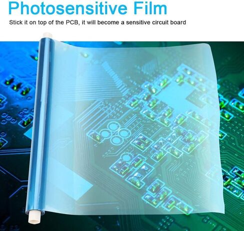
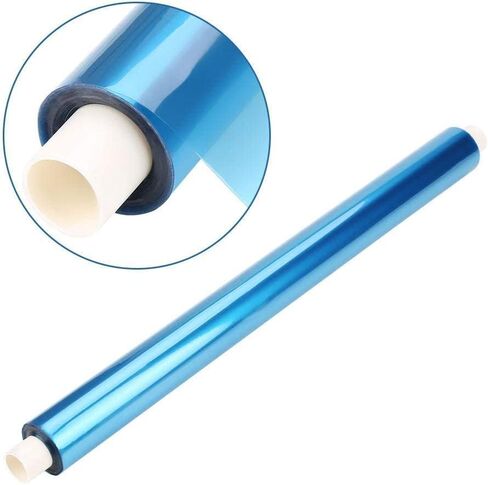
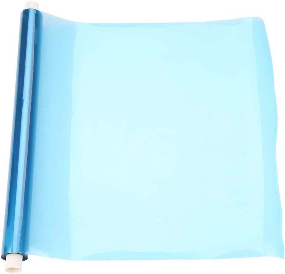
1. Uncover the film, the photosensitive film is sandwiched between two layers of film, first tear off one side, it is a bit difficult to tear off, just try a few more times
2. Then paste the film, the copper plate can be cleaned a little, and paste it flat, try not to have bubbles
3. After being pasted, the electric iron will heat up a little, not too hot, and will play a fixed role
4. For printing circuit board film, it is recommended to use film, which can achieve the highest degree of fineness. If there is no requirement for precision, use sulfuric acid paper for printing.
5. Exposure, put the printed pattern on the photosensitive plate, use an ordinary energy-saving lamp for about 30 minutes, if there is an exposure machine, it will do for 1 minute, and I have not tried it under the sun.
It should be about 15 minutes, the exposure process is obvious, because the photosensitive film will change color during exposure, from light color to dark blue. You will easily see your circuit diagram appear on the board.
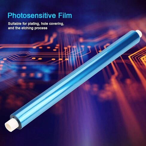
6. For developing, take off another protective film and put it in the developer (the developer should be mixed with water at 1:100, and 10 grams with 1 liter of water). Wipe the test board with a cotton swab while developing.
7. Etching, (ferric chloride, environmentally friendly etchant, hydrochloric acid + , etc.), water saturated solution of etchant
8. After etching, remove the film. Mix the release agent with water at 1:60 or 70, and soak the board for a few minutes.
Specification:
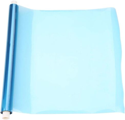
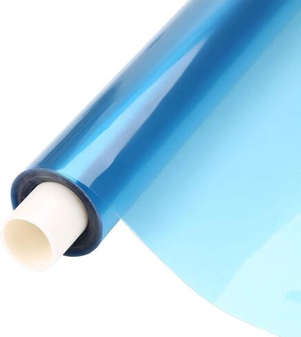
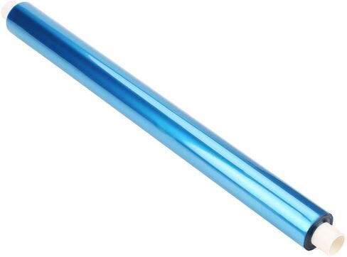
Material: Plastic
Dimension: 30cm*500cm / 11.8*197in
Weight: approx. 150g
Package List:
1 * Photosensitive Dry Film
 Sony UPC21S Print Pack S-Size Paper for the UP-21MD, UP23-MD, and UP-D25 MD Color Video Printers
KWD 63
Sony UPC21S Print Pack S-Size Paper for the UP-21MD, UP23-MD, and UP-D25 MD Color Video Printers
KWD 63
 KODAK FunSaver 35mm Single Use Camera
KWD 7
KODAK FunSaver 35mm Single Use Camera
KWD 7
 Memorablepix Instax Polaroid Mini Film Key Chain - Custom Picture Key Ring for Fujifilm Mini 9 Photo Film
KWD 3.500
Memorablepix Instax Polaroid Mini Film Key Chain - Custom Picture Key Ring for Fujifilm Mini 9 Photo Film
KWD 3.500
 Dubble Film Pacific 200 Color Negative Film (120 Roll, 2-Pack)
KWD 20.500
Dubble Film Pacific 200 Color Negative Film (120 Roll, 2-Pack)
KWD 20.500