- Shopping, made easy.
- /
- Get the app!
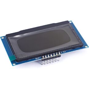
1.VCC:Power 2.GND:Power Ground 3.SCL:This pin is used to be serial interface clock 4.SDA:SPl interface input/output pin.the data is latched on the rising edge of the SCL signal. 5.DC:Display data/command selection pin in 4-line serial interface 6.CS:Chip selection pin;Low enable, high disable 7.RST:This signal will reset the device and it must be applied to properly initialize the chip.Signal is active low.
 Teyleten Robot D1 Mini ESP32 ESP-WROOM-32 WLAN WiFi+Bluetooth Internet of Things IoT Development Board for Arduino NodeMCU (3pcs)
KWD 8.500
Teyleten Robot D1 Mini ESP32 ESP-WROOM-32 WLAN WiFi+Bluetooth Internet of Things IoT Development Board for Arduino NodeMCU (3pcs)
KWD 8.500
 Teyleten Robot TCS34725 TCS-34725 Sensor Recognition Module RGB Sensor for Arduino (3pcs)
KWD 4.500
Teyleten Robot TCS34725 TCS-34725 Sensor Recognition Module RGB Sensor for Arduino (3pcs)
KWD 4.500
 Teyleten Robot 2.42 inch 128x64 OLED LCD Display Module SSD1309 7 Pin SPI/IIC I2C Serial Interface for Arduino UNO R3 - White Light
KWD 6.500
Teyleten Robot 2.42 inch 128x64 OLED LCD Display Module SSD1309 7 Pin SPI/IIC I2C Serial Interface for Arduino UNO R3 - White Light
KWD 6.500
 Teyleten Robot ESP32-S3-DevKitC-1-N16R2 ESP32-S3 Development Board Wi-Fi + BLE MCU Module Integrates Complete Wi-Fi and BLE Functions 3pcs
KWD 10.500
Teyleten Robot ESP32-S3-DevKitC-1-N16R2 ESP32-S3 Development Board Wi-Fi + BLE MCU Module Integrates Complete Wi-Fi and BLE Functions 3pcs
KWD 10.500


